Gallium Arsenide Wafers
This compound is synthetically produced for electronic industry due to its semiconductor properties.
Gallium Arsenide GaAs – an inorganic compound of gallium and arsenic.
The second one after silicon (Si) material most commonly used in micro- and optoelectronics and microwave technology.
Gallium arsenide shows greater electromagnetic radiation resistance than silicon.
GaAs electronic devices can operate at frequencies exceeding 250 GHz. Semiconductor parameter – energy interruption (at 300 K) = 1,424 eV.
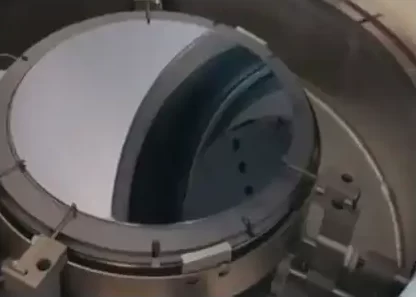
Wafers in our offer are produced from crystals using the VGF, LCP and Horizontal Synthesis method.
Liquid encapsulated Czochralski (LCP) – This method requires complicated equipment, because it creates a high pressure of arsenic vapor, but it allows to overcome many problems of gradual growth of this crystal.
Vertical Gradient Freeze (VGF) – the flagship method of producing GaAs wafer, provides a low dislocation density in the crystal.
Small quantities or individually packed wafers are available.
Galluim Arsenide wafer specifications
| Wafer diameter | 2ʺ-200 mm |
| Wafer thickness | 350µm – 635µm |
| Surface finishing | epitaxy – ready finishing |
| Crystal orientation | (100) (111) (110)… |
| Dopant | N-type, P-type or undoped |
| Dopant material | Zn, C, Te, Si… |
| Crystal growth | LEC (Liquid encapsulated Czochralski), VGF (Vertical Gradient Freeze) |
Should you need any further information or you are unable to find the wafer specification you require, please do not hesitate to contact us: info@waferexport.com or TOLL FREE in Spain (+34) 622 375 955, Portugal (+351) 800 180 183 or France +33 805 080 082.