Wafer Grinding Service
Wafer grinding, also known as wafer back-grinding or wafer thinning, is a finishing process of the surface by abrasive tools, which results in a thinning of the wafer with high accuracy and low roughness. Its purpose may vary according to the uses we may need for the device that we are fabricating, being the space optimization and the heat dissipation the main reasons why wafer grinding is such important in the semiconductor manufacturing process.
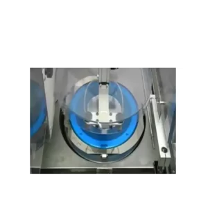
Machines for this type of processing are called grinders and their cutting tools, grinding wheels. These are usually made of corundum, diamond, silicon carbide or boron carbide.
The process usually involves several steps, thinning the wafer in each of them until the desired thickness is achieved. The typical silicon wafer thickness is around 750 μm once laminated from de silicon ingot, but through the process of grinding thickness down to 50 μm can be achieved.
Wafer grinding specifications
| Diameter | 100 – 300mm |
| TTV | As low as 2µm (before polishing) |
| Thickness | Can grind wafers as thin as 50µm |
Contact us to get a personalized quotation according to your needs. Should you need any further information, please do not hesitate to contact us too via email info@photonexport.com or by phone (toll free) in Spain +34 622 375 955, Portugal +351 800 180 183 or France +33 805 080 082.
More services we offer : Polishing, Etching, Dicing, Crystal Growth, Bonding.