Silicon Wafer Dicing Services
WaferExport offers a wide range of services including wafer dicing.
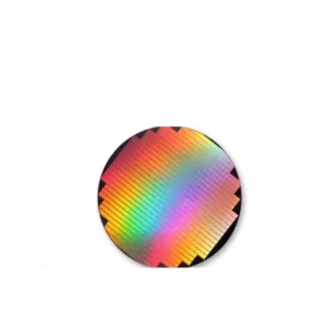
The dicing technique is part of semiconductor electronic circuit back-end manufacturing. During the front-end wafer manufacturing process, many integrated electronic circuits are made in a single wafer by depositing one or more thin film layers and shaping them using the lithography and etching techniques.
Once ready, every wafer can contain up to a thousand of independent integrated circuits, they need to be cut out. This is the back-end process. After testing the wafer, the single integrated circuits are separated using dicing techniques such as laser ablation or dicing saws.
This technique involves separating the wafer die from the semiconductor during production. The die can range from 35 mm to 0.1 mm square. In this process we can distinguish breaking, sawing, scribing and laser cutting. Once the wafers have been cut into small chips, they can be used in the electronics industry, such as cell phones, computers and many other devices.
Individual dies can not be handle because they are small and fragile, the dies are bonded to a substrate call carrier. After the Die Bond, the interface to each die is performed by bonding electrical wires.
The packaging process is finished with the encapsulating of the die and frame in a molded plastic, epoxies or protective coating.
Contact us to get a personalized quotation according to your needs. Should you need any further information, please do not hesitate to contact us too via email info@photonexport.com or by phone (toll free) in Spain +34 622 375 955, Portugal +351 800 180 183 or France +33 805 080 082.
More services we offer : Polishing, Grinding, Etching, Crystal Growth, Bonding.