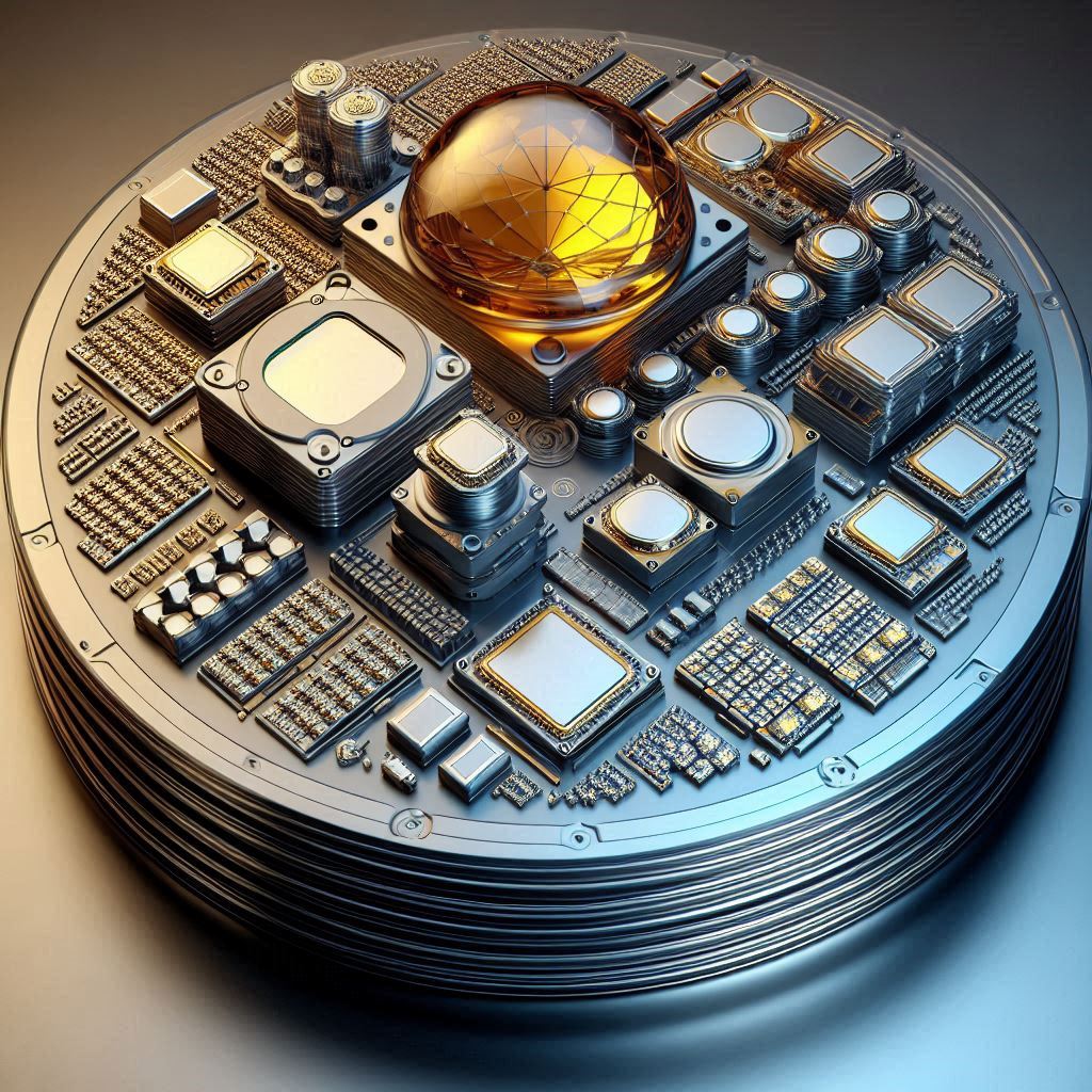
We offer SiC Wafers Research grade, Pirme grade and Epitaxial.

Silicon carbide (SiC) wafers are primarily available in two polytypes: 4H-SiC and 6H-SiC, each with unique characteristics suited for different applications in electronics and power devices. The choice between these polytypes depends on their electrical, structural, and thermal properties.
Key Differences Between 4H-SiC and 6H-SiC:
- Crystal Structure and Properties:
- 4H-SiC has a hexagonal structure with higher electron mobility and isotropic electrical properties, making it suitable for high-frequency and power-switching applications.
- 6H-SiC also has a hexagonal structure but offers higher hole mobility, often utilized in applications where such properties are advantageous.
- Applications:
- 4H-SiC is widely used in power devices like MOSFETs and Schottky diodes due to its superior electronic properties.
- 6H-SiC is commonly employed in optoelectronic devices and applications where lower cost is a consideration.
- Pricing:
- 4H-SiC wafers are generally more expensive because of their complex manufacturing process and superior performance characteristics.
Choosing the Right Grade:
- Prime Grade Wafers are premium quality with minimal defects, offering over 90% usable area and very low defect densities. They are ideal for critical applications in power electronics, EV powertrains, and aerospace.
- Research Grade Wafers are cost-effective and suitable for experimentation or less critical uses, offering slightly lower quality but higher affordability
Silicon Carbide (SiC) wafers are categorized into grades based on their quality, defect density, and intended applications. The most common grades include:
1. Epitaxial (Epi) Grade
- Description: These wafers have an epitaxial layer grown on the surface for electronic applications like MOSFETs, diodes, and power devices.
- Defect Density: Low micropipe density (≤1 cm⁻² or lower for premium grades).
- Typical Applications: High-power, high-frequency, and high-temperature electronics.
2. Prime Grade
- Description: High-quality wafers with minimal surface defects and uniform doping.
- Surface Quality: High polish with minimal scratches and defects.
- Typical Applications: Research and development, device fabrication.
3. Research Grade
- Description: Wafers with moderate defect density, suitable for prototyping and academic purposes.
- Defect Density: Moderate micropipe and defect density.
- Typical Applications: Experimental device development and academic research.
4. Dummy or Test Grade
- Description: Wafers with higher defect density or non-uniform doping. Used for calibration, testing, and non-critical experiments.
- Defect Density: High micropipe and defect density.
- Typical Applications: Equipment calibration and test runs.
5. Semi-Insulating Grade
- Description: Wafers with high resistivity, used for RF and microwave applications.
- Typical Resistivity: >10⁵ Ω·cm.
- Typical Applications: High-frequency devices like RF amplifiers.
6. Conductive (Doped) Grade
- Description: Doped SiC wafers with n-type (Nitrogen) or p-type (Aluminum or Boron) conductivity.
- Resistivity Range: Controlled doping for desired electrical characteristics.
- Typical Applications: Power electronics and optoelectronics.
7. Off-Axis or Angled Cut
- Description: Wafers cut at specific angles (e.g., 4°, 8°) relative to the crystal orientation to optimize epitaxial layer growth.
- Typical Applications: High-quality epitaxy and device fabrication.
Key Considerations for SiC Wafers:
- Micropipe Density: Critical for power applications; lower densities are preferred.
- Wafer Size: Common diameters include 2″, 4″, 6″, and emerging 8″.
- Polytype: The most common is 4H-SiC, suitable for high-performance devices.
- Orientation: Standard orientations include (0001) or (11-20), depending on the application.
Silicon carbide (SiC) wafers are primarily available in two polytypes: 4H-SiC and 6H-SiC, each with unique characteristics suited for different applications in electronics and power devices. The choice between these polytypes depends on their electrical, structural, and thermal properties.
Key Differences Between 4H-SiC and 6H-SiC:
- Crystal Structure and Properties:
- 4H-SiC has a hexagonal structure with higher electron mobility and isotropic electrical properties, making it suitable for high-frequency and power-switching applications.
- 6H-SiC also has a hexagonal structure but offers higher hole mobility, often utilized in applications where such properties are advantageous.
- Applications:
- 4H-SiC is widely used in power devices like MOSFETs and Schottky diodes due to its superior electronic properties.
- 6H-SiC is commonly employed in optoelectronic devices and applications where lower cost is a consideration.
- Pricing:
- 4H-SiC wafers are generally more expensive because of their complex manufacturing process and superior performance characteristics.
Choosing the Right Grade:
- Prime Grade Wafers are premium quality with minimal defects, offering over 90% usable area and very low defect densities. They are ideal for critical applications in power electronics, EV powertrains, and aerospace.
- Research Grade Wafers are cost-effective and suitable for experimentation or less critical uses, offering slightly lower quality but higher affordability
Example of 4H-SiC wafer
| Characteristic | Specification |
|---|---|
| Wafer Type | 4H-SiC |
| Diameter | 4 inches (100 mm) |
| Orientation | <0001> 4° off or <0001> ± 0.5° |
| Thickness | 350 µm ± 25 µm or 550 µm ± 25 µm |
| Conductivity Type | n-type |
| Dopant | Nitrogen (N) |
| Resistivity (Ro) | 0.012–0.030 Ω·cm |
| Micropipe Density (MPD) | <100 cm⁻² |
| FWHM (Full Width at Half Maximum) | <50 arcseconds |
| Polishing | Double-side polished; Epi-ready Si face polished |
| Surface Roughness | <0.5 nm |
FWHM (Full Width at Half Maximum): This parameter measures the crystalline quality of the wafer; lower values indicate better crystal perfection.
Surface Roughness: Important for epitaxial growth; roughness <0.5 nm ensures smooth surfaces.
Small quantities or individually packed wafers are available.
Should you need any further information or you are interested in other product parameters, please do not hesitate to contact us: info@waferexport.com or TOLL FREE in Spain+34 622 375 955 Portugal (+351) 800 180 183 or France +33 805 080 082.
Read about more products we offer: Silicon Wafer, Indium Phosphide , Thermal Oxide, SOI/SIlicon On Insulator, Silicon Nitride.
