Semiconductor Wafers Explained: Types, Orientation & Applications
A semiconductor wafer is a thin disc that can be made of different types of materials.
Most common wafers are made of Silicon, but other materials can also be used, for example compound III-V materials (GaAs, InP) or Sapphire.
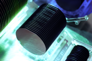
The circular shape of the wafer is given by its growth method.
A big rod is thinly sliced to form each wafer.
Importance of wafer crystal orientation
When slicing the rod, one aligns the surface in one of the relative directions known as crystal orientations. When working with crystal structured materials, orientation is relevant since for each orientation, electrical and mechanical properties may be different, because these properties are highly anisotropic (different properties in different directions).
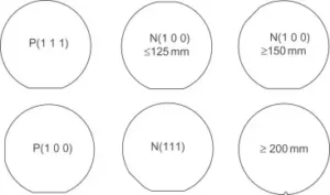
Flats and shape images
In case of Silicon wafers, depending on the crystallographic orientation, a series of flats are required at a specific position to distinguish each type of wafer, as follows:
Applications
The range of applications of a wafer is wide and it depends on the substrate. Most used semiconductors in the production of microchips and chips for electronic devices are silicon wafers. Semiconductors, essential for constructing integrated circuits, utilize the unique properties of electrical current flow within silicon wafers. Silicon, abundant and cost-effective, possesses a bandgap of approximately 1.1 eV, making it ideal for electronic devices. This optimal bandgap value enables semiconductor-based technologies to operate efficiently and perform effectively.
GaAs (gallium arsenide) exhibits a wider band gap than silicon. Additionally, compared to silicon, there is more electron mobility (1000 cm^2/V*s in Si and 9000 cm^2/V*s in GaAs, when measured at 300 K). For those reasons, GaAs is used in semiconductors, lasers, photovoltaic cells, tunneling diodes, and MESFET (not MOSFET) transistors.
Sapphire wafers are extensively used in LED manufacturing.
Other shapes of wafers
As the growth method implies, the shape of the wafers is mostly circular, but some other shapes of wafers are commercialized. We can find square or rectangular shapes for sapphire substrate wafers, for example.