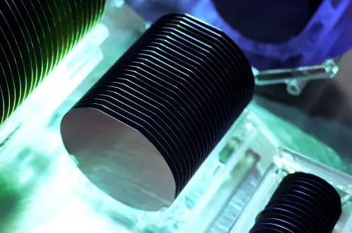
The Production Processes of Silicon Wafers
The production of silicon wafers, essential elements in electronic device manufacturing, relies on several sophisticated methods. These methods, such as the Czochralski method, the floating zone process, and others, play a crucial role in creating high-quality semiconductor materials. Join us as we explore the various stages of silicon wafer production.
Czochralski method (CZ)

The CZ method is one of the most common approaches for growing single-crystal silicon ingots. In this method, high-purity semiconductor material is melted in a crucible, and dopants can be introduced if needed. A seed crystal is then immersed in the molten semiconductor, forming a large cylindrical single-crystal ingot through controlled pulling and rotation. Advantages of the CZ method include its ability to produce large single-crystal ingots crucial for the electronics industry. However, challenges may arise in controlling variables such as temperature gradients, pulling speeds, and rotational speeds, potentially hindering optimal crystal growth. The CZ method primarily finds application in growing large cylindrical monocrystalline silicon blocks, essential in semiconductor device production. This method play an important role in the production process of Silicon wafer .
Float Zone Method (FZ)
The Float Zone (FZ) method is another effective technique for crystal growth, particularly for producing purer crystal ingots. In this method, a single crystal is grown by immersing one end of a seed crystal in a specific area, and the growing process requires pulling out the seeds. The main advantage of the FZ method is that no crucible is required, thus reducing impurities and crystal defects. However, challenges may arise in controlling the growth process without using crucibles, requiring precise management of variables. Floating zone technology finds important applications in power devices, detectors requiring high resistivity, and the growth of refractory materials, particularly where avoiding crucible problems is crucial.
Vertical Gradient Freeze Method (VGF)
The Vertical Gradient Freeze (VGF) method is commonly used for growing III-V compound crystals like GaAs, InP, or GaP. This method involves heating and melting a polycrystalline raw material containing seed crystals in a crucible, facilitated by resistive heating.
Then, the temperature zone or crucible gradually cools the melt to induce solidification, with precise control of the crystallization rate linked to adjusting the movement of the temperature zone during cooling. The VGF method offers the advantage of producing crystals with low dislocation density, particularly in materials critical for semiconductor applications.
However, challenges may arise in accurately controlling the crystallization rate, necessitating careful management of cooling process variables. This method can produce crystals of gallium arsenide (GaAs), indium phosphide (InP), or gallium phosphide (GaP), meeting the stringent requirements for semiconductor materials in electronic device manufacturing.
Heat Exchange Method
The Heat Exchange method, similar to the Kyropoulos method, is used for growing sapphire crystals. This method uses a heat exchanger to dissipate heat and create a longitudinal temperature gradient in the crystal growth area. Precise control of gas flow and adjustment of heating power help maintain the gradient and achieve slow crystal growth from bottom to top. The method’s focus on temperature control plays a crucial role in achieving the desired crystal quality.
One advantage is the ability to produce sapphire of the highest quality. However, the method’s complexity and higher cost pose challenges, making it less economical than other methods. This process yields excellent sapphire, ideal for applications needing high power, UV properties, or strict specifications such as high power thresholds and zero fluorescence. However, its limited usage is due to its higher cost and development challenges, making it better suited for specific applications.
Horizontal Bridgman Method
The Bridgman method, employed for growing III-V compound crystals, allows for both vertical and horizontal layouts. This method utilizes a container to hold the polycrystalline material, heated beyond its melting point. Controlled cooling enables the continuous development of single-crystal material along the container’s length. A seed crystal is placed at one end, initiating the process.
Precise control over the temperature gradient at the melt/crystal interface allows for the production of high-quality semiconductor crystals. However, maintaining consistent conditions throughout the lengthy cooling process may pose challenges. The Bridgman method is widely utilized in semiconductor crystal production, particularly for materials like gallium arsenide. It ensures critical crystal quality through accurate temperature gradient control at the melt/crystal interface.
Kyropoulos Method
The Kyropoulos method is used by some companies to produce sapphire crystals for the electronics and optics industry. This method involves adding a seed into the semiconductor that has melted in a crucible. As the seed is cooled with the help of a seed holder, efficient heat exchange from the furnace occurs, facilitating crystal formation. Another approach involves controlled development by lowering the crucible through a thermal gradient.
Temperature adjustments are made to achieve optimal outcomes in this method. The excellent optical qualities make this approach suitable for a wide range of optical applications. However, it is not suitable for situations requiring excessive power thresholds or prolonged exposure to intense UV radiation. The Kyropoulos method is preferred in high-purity applications such as semiconductor and LED production. However, it may not be ideal for applications with strict power threshold and UV requirements.
